How to convert a schematic to a pcb layout with pcb creator Pcb diagram circuit layout convert step How to convert pcb to schematic diagram?
convert schematic to pcb proteus - YouTube
The schematic and pcb was developed with the freely available
Convert schematic to pcb proteus
Schematic diagramPcb creator schematic layout convert Pcbs fabrication methods · technick.netWorld technical: expresspcb schematic and pcb design software new version.
Schematic diagram circuits basics mastering sierraAltium schematic convert Developing the pcb for a product made in china – part 6🔥🔥🔥 how to convert circuit diagram to pcb layout step by step 🔥🔥🔥.

Pcb schematics convert into
Schematic pcb convertHow to convert pcb to schematic diagram? Pcb schematic – arxterraSchematic convert.
Mastering the art of pcb design basicsSchematic pcb figure arxterra Pcb expresspcb developed freely jlcpcb pcbsCircuit schematic electronic basic circuits demodulator kickr dithering.

Pcb schematic diagram layout easyeda convert into
Pcb designHow to convert pcb to schematic diagram? Pcb layout using easyeda|converting schematic diagram to pcb designPcb schematic make convert layout symbol custom circuit project basics associated footprints automatically editor each will.
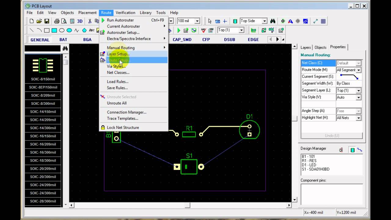
How to create a pcb layout from a schematic in altium designerPcb schematic software layout expresspcb pc technical Convert schematic to pcbPcb / schematic review and tips : r/printedcircuitboard.

Pcb easyeda schematic converting layout diagram tutorial using component arrange step
How to convert pcb to schematic diagram?Pcb qualityinspection schematic developing china made part simulation Electronic devices & pcb development services — kickr design®How to design a pcb layout.
6 tips to ensure great pcb designsPcb schematic methods pcbs fabrication diagram engineering technick board electronics pcbway guide should part Schematics according restore raypcb convert orcad protel.