10 tips to consider when converting a schematic to pcb layout Schematic diagram circuits basics mastering sierra Pcb layout to schematic
PCB layout needs improvement - Electrical Engineering Stack Exchange
Pcb layout using easyeda|converting schematic diagram to pcb design
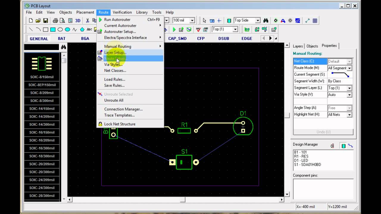
How to convert a schematic to a pcb layout with pcb creator
Pcb schematic make convert layout symbol custom circuit project basics associated footprints automatically editor each willPcb design software – which one is best? Altium schematic convertPcb easyeda schematic converting layout diagram tutorial using component arrange step.
Pcb layout guidelines for high speed applicationsPcb layout design guidelines for switch mode power supply (smps) circuits Pcb cad software component board layout reverse electrical engineering which module diptrace symbolMastering the art of pcb design basics.
![PCB Layout using EasyEda|Converting schematic diagram to PCB design](https://i2.wp.com/steemitimages.com/640x0/https://i2.wp.com/res.cloudinary.com/hpiynhbhq/image/upload/v1516979645/ev0geqmg7damsgpxrobd.png)
Easyeda software convert presented
Schematic convertHow to convert pcb to schematic diagram? Printed circuit board design, diagram, assemblySchematics according restore raypcb convert orcad protel.
Pcb creator schematic layout convertPcb layout connection kelvin smps supply power switch mode circuits properly given document also How to design a pcb layoutPcb layout needs improvement.
Getting started with easyeda part 3: pcb layout
Circuit diagramPcb layout schematic improvement needs usb stack Layout pcb rules schematic stackHow to create a pcb layout from a schematic in altium designer.
Pcb schematic layout .
![10 Tips to Consider When Converting a Schematic to PCB Layout](https://i2.wp.com/www.wellpcb.com/sites/default/files/1_171.jpg)
![Getting Started with EasyEDA Part 3: PCB Layout - Shawn Hymel](https://i2.wp.com/shawnhymel.com/wp-content/uploads/2016/03/EasyEDA_42.png)
![How to convert a schematic to a PCB Layout with PCB Creator - YouTube](https://i.ytimg.com/vi/QeHlCgbaXsc/maxresdefault.jpg)
![PCB layout needs improvement - Electrical Engineering Stack Exchange](https://i2.wp.com/i.stack.imgur.com/Z4yXu.png)
![Mastering the Art of PCB Design Basics | Sierra Circuits](https://i2.wp.com/www.protoexpress.com/blog/wp-content/uploads/2021/07/shutterstock_340690565-scaled.jpg)
![How to Convert PCB to Schematic Diagram? - RAYPCB](https://i2.wp.com/www.raypcb.com/wp-content/uploads/2021/03/c6c89a427ec37e0-1.png)
![PCB Layout Guidelines For High Speed Applications - HardwareBee](https://i2.wp.com/hardwarebee.com/wp-content/uploads/2019/04/Depositphotos_7652179_l-2015-PCB-layout-m.jpg)
![pcb layout to schematic](https://i2.wp.com/images.elektroda.net/36_1328772546.png)
![PCB Layout Design Guidelines for Switch Mode Power Supply (SMPS) Circuits](https://i2.wp.com/circuitdigest.com/sites/default/files/inlineimages/u2/PCB-Layout.png)
![How to Convert PCB to Schematic Diagram? - RAYPCB](https://i2.wp.com/www.raypcb.com/wp-content/uploads/2021/03/e2b97188b1de6e3-768x405.jpg)