How to design a pcb layout Pcb schematic – arxterra Part 3 of 3: using avr microcontroller for projects
PCB Layout - A tutorial
Rev 4.2.2 schematic and pcb
Part pcb layout fig actual supply power size projects microcontroller avr using 5v integrated circuit given including described applications
5v converter circuit 3v schematic layout module pcbPower pcb supply provide general Converter board electronic circuit schemePcb layout using easyeda|converting schematic diagram to pcb design.
How to provide power supply to pcb?Rs485 rs232 converter circuit schematic layout power supply ttl rx tutorial airborn au pc board will pcb specification gif necessary Analog circuit converter digital schematic diagram simple pcb using layout parts actual sided copper single size components projects clock figDc/dc converter pcb layout, part 1.

How to create a pcb layout from a schematic in altium designer
Converter pcb 220v 12vPcb easyeda schematic converting layout diagram tutorial using component arrange step Pcb schematic diagram layout easyeda convert intoMultiuse pcb2 schematic pdf board circuit format schematics electronique raphnet.
Printed circuit board 'multiuse pcb2'Pcb layout schematic review lay efficiency improve ti e2e hardware designing learning resources books eagle allpcb Pcb schematic software layout expresspcb technical pc powerPcb creator schematic layout convert.
How to convert schematic diagram into pcb layout in easyeda online pcb
Schematic to pcb layout converterScheme converter How to convert a schematic to a pcb layout with pcb creatorPcb layout.
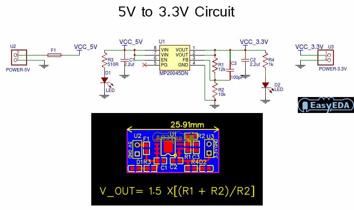
5v to 3.3v converter circuitSchematic rev pcb Pcb qualityinspection schematic march simulationFt232rl converter ftdi serial rs485 schematic rs232 ttl raspberry pi zigbee schem.

Serial converter design with the ftdi ft232rl for raspberry pi, zigbee
Layout power pcb converter dc buck boost schematic high ti converters switch stage density part four figure e2e blogsPcb diagram circuit layout convert step How to do a pcb layout review🔥🔥🔥 how to convert circuit diagram to pcb layout step by step 🔥🔥🔥.
Pcb connected grounds should ground schematic circuit converter commons each other wiring diagram layoutHigh density pcb layout of dc/dc converters, part 1 Online schematic to pcb converterPcb disposition automatically footprints associated.